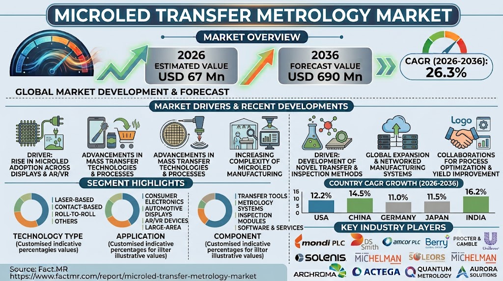
The global MicroLED Transfer Metrology Market is projected to grow from USD 67 million in 2026 to USD 690 million by 2036, advancing at a 26.3% CAGR during the forecast period. The market was valued at USD 53.0 million in 2025, creating an absolute opportunity of approximately USD 623 million through 2036.
MicroLED manufacturing requires accurate measurement of transferred emitters before defects move into later assembly stages. Display makers need faster feedback on missing or shifted dies, while panel OSATs require coordinate data across mass-transfer and repair workflows. Equipment manufacturers are also integrating inspection data with transfer tools to help identify placement errors earlier in production. The U.S. Census Bureau reported on July 27, 2026, that June 2026 new orders for computers and electronic products reached USD 31.1 billion, supporting adjacent demand for electronics process-control equipment.
Get Detailed Market Forecasts, Competitive Benchmarking, and Pricing Trends
Global Segment Leaders
- High-speed optical imaging accounts for 43.0% of the market by metrology technique in 2026. Its position is supported by the need for rapid die-position feedback and visual defect review within production lines.
- Placement accuracy represents 34.0% of the measured-parameter segment. Precise emitter positioning is critical before bonding, inspection, and repair activities begin.
- Inline high-throughput systems hold a 57.0% share by throughput class. These systems help identify transfer errors during production instead of waiting until costly rework stages.
- Micro-displays and AR account for 36.0% of the display-type segment. High pixel density and tight viewing distances increase the need for precise optical verification.
- Display makers lead the end-user segment with a 48.0% share. These companies directly manage panel yield and need transfer data connected with inspection and repair processes.
Country-Level Performance
- Poland: The market is projected to expand at a 33.8% CAGR through 2036. Semiconductor-sector policy and investment in infrastructure, financing, workforce, and education are supporting the country’s developing semiconductor ecosystem. Poland’s Ministry of Digital Affairs finalized its semiconductor-sector policy on June 18, 2025.
- Finland: A 33.0% CAGR is forecast through 2036. Photonics, microelectronics, and quantum technology programs are creating opportunities for early metrology trials. Business Finland’s Chips Campaign lists a EUR 40 million funding target for these areas.
- United Kingdom: The market is expected to advance at a 31.3% CAGR. Semiconductor clusters and compound-device development are supporting demand, with the UK’s 2026 Semiconductor Sector Study identifying 705 semiconductor companies.
- South Korea: A 30.7% CAGR is anticipated through 2036. The country’s established display manufacturing base and equipment ecosystem support access to specialized development and qualification networks. South Korea’s ICT exports reached USD 264.3 billion in 2025, up 12.4% year over year.
- Germany: The market is projected to grow at a 30.0% CAGR. Industrial electronics, optics, and precision-equipment capabilities are supporting adoption. Germany recorded a 7.8% increase in manufacturing orders in December 2025, while electrical equipment orders rose 9.8%.
- USA: The market is forecast to expand at a 22.2% CAGR. Semiconductor packaging investment is creating adjacent demand for placement and inspection technologies. The U.S. Department of Commerce finalized USD 1.4 billion in awards for next-generation semiconductor advanced packaging in January 2025.
- Japan: A 20.8% CAGR is projected through 2036. Japan’s equipment and measuring-instrument capabilities support demand for precision inspection technologies. JEITA reported 2025 production of JPY 3,416,604 million for industrial electronic equipment and JPY 523,884 million for electric measuring instrumentation.
Market Drivers and Opportunities
Mass-transfer yield control remains the strongest identified growth driver, with an estimated +2.5% impact on CAGR. Detecting shifted or missing dies earlier can help reduce yield losses before panels reach module assembly.
AR and micro-display pixel density has an estimated +1.8% impact on CAGR. Small pixels make placement and color variations more visible, increasing the need for coordinate accuracy and optical uniformity checks.
Inline inspection and repair-loop integration contributes an estimated +1.5% impact on CAGR. Production lines increasingly need inspection data that can move directly into repair decisions rather than requiring separate manual review.
Among emerging opportunities, closed-loop transfer and repair maps carry an estimated +1.4% impact on CAGR. These systems connect placement coordinates with repair commands and can help process engineers trace defects to specific production steps.
Micro-display process qualification is another opportunity, particularly for AR and wearable programs that require repeatable inspection across small pixel layouts. Panel-level metrology and photonics-related transfer applications also provide longer-term opportunities.
High qualification costs remain a restraint, with an estimated -0.8% impact on CAGR. Limited MicroLED production scale, cautious display capital expenditure, and shortages of specialized tool skills may also slow adoption.
Competitive Landscape
The competitive environment includes Toray Engineering Co., Ltd., Onto Innovation Inc., V Technology Co., Ltd., Camtek Ltd., and KLA CORPORATION. Competition is centered on inline inspection speed, coordinate repeatability, defect classification, and integration of metrology data with transfer and repair workflows.
Toray Engineering reported in August 2025 that it had developed bonding technology for ultra-thin semiconductors aimed at high-throughput mass production of advanced semiconductors and next-generation photonic integrated circuits. The company has the clearest MicroLED transfer fit identified in the report.
Onto Innovation launched the Dragonfly G5 inspection system on March 16, 2026, with defect sensitivity down to 150 nm. Its inspection and metrology capabilities also extend into advanced packaging applications.
KLA has direct MicroLED mass-transfer inspection and metrology evidence through its Orbotech Flare MT Inspection and Metrology offering, while V Technology contributes established display-equipment capabilities. Camtek is positioned as an adjacent inspection and metrology supplier with strengths across semiconductor wafer, panel, and advanced-packaging inspection.
Other Related Reports:
Multi-Chamber Biobased Detergents Market
Aviation Component Digital Twins Market
Analyst Perspective
Shambhu Nath Jha, Principal Consultant at Fact.MR, states:
“Transfer metrology is becoming a yield-control layer, not a final inspection step. Suppliers are expected to gain attention when optical imaging, coordinate measurement and repair-loop data are connected inside the production line. The better platforms combine speed, placement traceability and defect classification in a format trusted by process engineers.”
The report covers optical imaging, photoluminescence mapping, and electroluminescence testing, with applications spanning micro-displays, wearables, large-format displays, and automotive displays. The analysis draws on 120+ sources, 35+ company portfolios, 25+ countries, and more than 20 industry interviews.