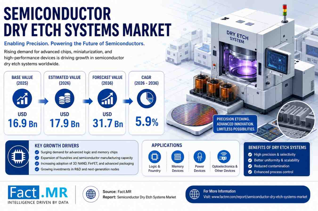
The global semiconductor dry etch systems market was valued at USD 16.90 billion in 2025, is estimated at USD 17.90 billion in 2026, and is projected to reach USD 31.75 billion by 2036. According to a detailed market analysis published by Fact.MR, the industry is expected to expand at a compound annual growth rate (CAGR) of 5.9% over the 2026 to 2036 forecast period.
Get detailed market forecasts, competitive benchmarking, and pricing trends: https://www.factmr.com/connectus/sample?flag=S&rep_id=11699
For semiconductor fab procurement leads, equipment category managers, foundry technology directors, and microelectronics investors, dry etching equipment remains a core capital expenditure priority required to enable sub-3nm chip production and advanced 3D device architectures.
Key Market Highlights at a Glance
- Base Year Valuation (2025): USD 16.90 billion
- Estimated Market Size (2026): USD 17.90 billion
- Forecast Market Size (2036): USD 31.75 billion
- Absolute Dollar Opportunity (2026–2036): USD 13.85 billion
- Compound Annual Growth Rate (CAGR):9% from 2026 to 2036
- Leading Etching Technique Segment: Deep Reactive Ion Etching (DRIE) capturing 46.8% market share in 2026
- Leading Application Segment: Logic and Memory accounting for 42.7% market share in 2026
- Fastest-Growing Country Market: China expanding at a 7.6% CAGR through 2036
Why Is the Semiconductor Dry Etch Systems Market Growing?
Demand for semiconductor dry etch systems is expanding steadily due to the global rush toward chip miniaturization, 3D wafer stacking, and high-density semiconductor fabrication. As traditional wet etching reaches physical limits in micro-patterning, semiconductor foundries rely on plasma-based dry etching to achieve nanoscale precision.
- Transition to Gate-All-Around (GAA) and Advanced Nodes: Fabs manufacturing sub-3nm logic chips require atomic-level plasma etching accuracy to sculpt complex transistor structures without damaging underlying layers.
- Rapid Expansion of 3D Memory Architectures: The commercial scaling of high-density DRAM and multi-layer 3D NAND flash devices demands deep, high-aspect-ratio trench etching capabilities.
- Government Fab Incentives and Regionalization: Initiatives like the U.S. CHIPS Act and India’s USD 9.2 billion Semicon India Program are incentivizing new fab construction and capital spending on front-end processing tools.
“Dry etching technology is the critical enabling tool for next-generation microelectronics,” noted Ganesh Pai, Lead Technology Analyst at Fact.MR. “As semiconductor foundries move beyond traditional FinFET designs toward Gate-All-Around architectures and high-density 3D memory, the ability to control plasma etching at atomic scales dictates yield rates and overall chip efficiency.”
Which Etching Technique and Application Segments Lead the Market?
By etching technique, the market is segmented into Deep Reactive Ion Etching (DRIE), Reactive Ion Etching (RIE), Inductively Coupled Plasma (ICP), and Atomic Layer Etching (ALE). Deep Reactive Ion Etching holds the dominant position, accounting for 46.8% of total revenue in 2026. DRIE leads because it provides high aspect ratio patterning essential for silicon via formation, MEMS fabrication, and complex 3D chip structures.
By application, the market is categorized across logic and memory, MEMS and sensors, and power devices. Logic and memory is the largest application segment, representing 42.7% of market share in 2026. High-volume fabrication of advanced processors, AI accelerators, and high-bandwidth memory (HBM) modules drives continuous procurement of multi-chamber dry etch systems.
- Deep Reactive Ion Etching (DRIE): Commands 46.8% market share in 2026 by enabling deep trenching and high-aspect-ratio silicon etching.
- Reactive Ion Etching (RIE): Maintains a strong baseline share across standard planar wafer processing and dielectric layer patterning.
- Logic and Memory Application: Accounts for 42.7% market share in 2026 due to surging demand for logic processors and 3D memory devices.
- Power Devices Application: Experiencing rapid growth propelled by Silicon Carbide (SiC) and Gallium Nitride (GaN) semiconductor manufacturing for electric vehicles.
What Are the Key Market Dynamics Shaping Industry Expansion?
Key Market Drivers
The primary growth driver for semiconductor dry etch systems is the proliferation of artificial intelligence, 5G telecommunications, and automotive electronics. These applications require high-performance, power-efficient microchips, driving foundries to upgrade their processing lines with high-throughput multi-chamber cluster etch tools.
Key Market Restraints
High initial capital equipment expenditure presents a major restraint for smaller foundries and research facilities. Furthermore, managing specialty process gases, maintaining plasma chamber uniformity over millions of cycles, and navigating strict international trade controls create operational friction for global fab operators.
Key Market Trends
A key industry trend is the increasing adoption of Atomic Layer Etching (ALE) for precise layer-by-layer material removal. Additionally, tool manufacturers are integrating artificial intelligence and real-time optical emission spectroscopy to monitor plasma health and optimize wafer yield automatically.
Regional Outlook: China Leads Growth, Followed by Emerging Asian and Western Markets
Asia-Pacific remains the world’s primary semiconductor manufacturing hub, driving major demand for front-end equipment. China is projected to be the fastest-growing national market for semiconductor dry etch systems, expanding at a CAGR of 7.6% through 2036. India is also emerging rapidly, posting a 7.0% CAGR driven by domestic fab ecosystem development.
- China: Forecast to achieve a 7.6% CAGR through 2036, driven by aggressive domestic semiconductor self-sufficiency investments.
- India: Projected to grow at a 7.0% CAGR, supported by state-level semiconductor assembly and fab subsidies.
- Germany: Set to advance at a 6.5% CAGR, supported by European automotive power electronics manufacturing.
- Brazil: Expected to expand at a 5.9% CAGR, driven by industrial electronics and assembly infrastructure growth.
- United States: Forecast to grow at a 5.3% CAGR, propelled by federal CHIPS Act subsidies and domestic foundry construction.
- United Kingdom: Anticipated to post a 4.8% CAGR, led by compound semiconductor research and specialty fab operations.
- Japan: Projected to grow at a 4.2% CAGR, grounded by established memory fab maintenance and equipment upgrades.
In China, expanding production of power semiconductors and legacy-node logic chips is driving continuous dry etch equipment orders. In India, foreign direct investment and government incentives are building a local semiconductor supply chain. In Germany and the United States, automotive electrification and re-shoring of advanced node manufacturing ensure sustained capital spending on cluster tool etching platforms.
Who Are the Key Players in the Semiconductor Dry Etch Systems Market?
The competitive landscape is concentrated among established semiconductor equipment manufacturers and rising regional suppliers. Leading vendors focus on multi-chamber cluster tool platforms, automated chamber cleaning, and advanced plasma density controls.
- Applied Materials, Inc.: Provides industry-standard plasma etch platforms designed for high-volume logic and memory pattern fabrication.
- Lam Research Corporation: Specializes in high-aspect-ratio dielectric and conductor dry etch systems for 3D NAND and advanced logic nodes.
- Tokyo Electron Limited (TEL): Offers high-precision plasma etch tools, including the Impressio and Tactras series, for advanced wafer processing.
- Hitachi High-Tech Corporation: Delivers microwave electron cyclotron resonance (ECR) plasma etch systems for sub-nanometer etching precision.
- Oxford Instruments plc: Supplies specialized atomic layer etching and plasma processing tools for compound semiconductors and research facilities.
- Plasma-Therm: Develops flexible plasma etch solutions for wireless, power device, and MEMS manufacturing applications.
- NAURA Technology Group Co., Ltd.: Manufactures ICP and DRIE equipment targeting expanding domestic semiconductor foundries in Asia.
- Advanced Micro-Fabrication Equipment Inc. (AMEC): Produces dielectric and conductor etch tools for advanced logic and memory production lines.
Market leaders are accelerating investments in Atomic Layer Etching technologies to address sub-2nm node challenges. Fabs are increasingly choosing equipment vendors that offer integrated process control software and predictive maintenance diagnostics to maximize tool uptime.
Read the Comprehensive Industry Report: https://www.factmr.com/report/semiconductor-dry-etch-systems-market
Frequently Asked Questions
What is the projected market size of the semiconductor dry etch systems market by 2036?
The global semiconductor dry etch systems market size is projected to reach USD 31.75 billion by 2036, growing from USD 17.90 billion in 2026.
What is the compound annual growth rate (CAGR) of the semiconductor dry etch systems market?
The semiconductor dry etch systems market is expected to expand at a compound annual growth rate (CAGR) of 5.9% between 2026 and 2036.
Which etching technique segment dominates the semiconductor dry etch systems market?
Deep Reactive Ion Etching (DRIE) is the leading etching technique segment, capturing a 46.8% market share in 2026.
Which application segment commands the largest market share for semiconductor dry etch systems?
The logic and memory application segment commands the largest share of the market, accounting for 42.7% of total revenue in 2026.
Which country is the fastest-growing market for semiconductor dry etch systems?
China is the fastest-growing national market for semiconductor dry etch systems, projected to expand at a 7.6% CAGR through 2036.
How much absolute dollar opportunity will the semiconductor dry etch systems market generate between 2026 and 2036?
The semiconductor dry etch systems market will generate an absolute dollar opportunity of USD 13.85 billion between 2026 and 2036.
Who are the key players in the semiconductor dry etch systems market?
Major players in the market include Applied Materials Inc., Lam Research Corporation, Tokyo Electron Limited, Hitachi High-Tech Corporation, Oxford Instruments, Plasma-Therm, NAURA Technology Group, and AMEC.
To View Related Report:
Semiconductor Defect Inspection Equipment Market: https://www.factmr.com/report/semiconductor-defect-inspection-equipment-market
Semiconductor Epoxy MOF Emissions Capture Market: https://www.factmr.com/report/semiconductor-epoxy-mof-emissions-capture-market
Semiconductor & Electronic Part Market: https://www.factmr.com/report/semiconductor-and-electronic-part-market
3nm Semiconductor EDA AI Tools Market: https://www.factmr.com/report/3nm-semiconductor-eda-ai-tools-market
Read the Comprehensive other Reports: