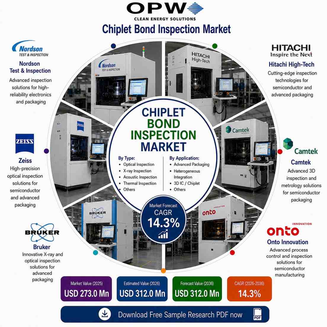
According to a comprehensive market research report published by Fact.MR, The global Chiplet Bond Inspection Market crossed a valuation of $273.0 million in 2025 and is projected to expand from $312.0 million in 2026 to $1.185 billion ($1,185.0 million) by 2036, recording a compound annual growth rate (CAGR) of 14.3% over the forecast period. This rapid adoption represents an absolute dollar opportunity of $873.0 million over the next decade.
Get detailed market forecasts, competitive benchmarking, and pricing trends: https://www.factmr.com/connectus/sample?flag=S&rep_id=15660
Market growth is primarily driven by outsourced assembly and test (OSAT) providers and foundries scaling 2.5D, 3D, and heterogeneous chiplet packaging workflows, where detecting buried voids, delamination, and sub-micron joint flaws without sacrificing high-value assemblies is essential to maintaining production yield.
Key Chiplet Bond Inspection Market Highlights at a Glance
- Base Year Market Valuation (2025): $273.0 million
- Estimated Market Value (2026): $312.0 million
- Forecast Market Value (2036): $1.185 billion ($1,185.0 million)
- Compound Annual Growth Rate (2026–2036):3%
- Absolute Dollar Opportunity (2026–2036): $873.0 million
- Leading Inspection Technique: Scanning acoustic microscopy (C-SAM) holding a 30.0% market share in 2026
- Leading Defect Type Segment: Interface voids capturing a 49.6% market share in 2026
- Leading Inspection Stage Segment: Post-bond inline inspection with a 47.3% market share in 2026
- Leading End-User Segment: OSAT providers commanding a 33.7% market share in 2026
- Fastest-Growing National Market: Taiwan expanding at a 15.6% CAGR from 2026 to 2036
Why Is the Chiplet Bond Inspection Market Growing?
Demand for chiplet bond inspection equipment is escalating as semiconductor packaging migrates from monolithic dies to complex multi-chiplet modules. Three primary industry drivers are accelerating tool adoption across commercial packaging facilities:
- Prevention of Downstream Value Destruction: Inspecting chiplet interfaces immediately after bonding prevents bad assemblies from receiving costly underfill, encapsulation molding, or additional die stacks.
- Detection of Buried Interface Defects: Multi-layer die stacks conceal internal joint voids, micro-cracks, and delamination that standard optical surface inspection tools cannot detect.
- Shift to Multi-Modal Non-Destructive Testing: High-volume advanced packaging lines require coordinated acoustic, X-ray, and infrared inspection flows to identify sub-micron bond flaws without destroying expensive substrates.
“Chiplet inspection will increasingly rely on coordinated acoustic, X-ray, infrared, and optical checks to identify buried defects without sacrificing costly multi-die assemblies,” states Ganesh Pai, Lead Semiconductor Analyst at Fact.MR. “As packaging facilities scale multi-die integration, discovering a bond defect post-bonding rather than post-molding provides immediate process feedback before downstream value accumulates across the module.”
How Does the Market Break Down Across Major Segmentation Axes?
Inspection Technique: Why Scanning Acoustic Microscopy (C-SAM) Leads
Scanning acoustic microscopy is projected to account for a leading 30.0% market share in 2026. Acoustic imaging uses high-frequency ultrasound reflection to screen entire wafer and die interfaces rapidly, providing micrometer-class lateral resolution to detect buried air voids, unbonded areas, and interfacial delamination.
- Scanning acoustic microscopy market share in 2026: 30.0%
- Primary process advantage: Delivers high-throughput, non-destructive screening of acoustic impedance changes at buried interfaces
- Key alternate segments: 3D X-ray/CT inspection for volumetric void distribution, 2D X-ray for gross bridging, and IR transmission metrology
Defect Type: Why Interface Voids Command Primary Focus
Interface voids are forecast to represent 49.6% of the defect type market segment in 2026. Voids directly reduce contact area across copper-to-copper pads and dielectric bonds, impeding thermal dissipation and driving mechanical cracking under operating temperature cycles.
- Interface voids market share in 2026: 49.6%
- Primary process impact: Uncovered voids reduce electrical contact area and act as stress concentration sites during thermal cycling
- Key alternate defect targets: Delamination, micro-cracks, and lateral placement misalignment
Inspection Stage: Why Post-Bond Inline Inspection Dominates
Post-bond inline inspection is projected to hold a 47.3% market share in 2026. Conducting inline acoustic or X-ray verification immediately following the bonding step allows automated systems to flag defective bonds before subsequent process steps compound manufacturing costs.
- Post-bond inline inspection market share in 2026: 47.3%
- Primary process advantage: Catches defective interfaces before underfill dispensing, molding, or final electrical testing add cost
- Secondary stage segment: Sampling and offline failure analysis tools used for process development and qualification
End User: OSAT Providers Driving Tool Procurement
OSAT providers are forecast to lead the end-user segment with a 33.7% market share in 2026. OSAT facilities integrate heterogeneous dies from multiple foundry sources and bear direct financial responsibility for yield loss when defective bond interfaces escape undetected into final modules.
- OSAT providers end-user market share in 2026: 33.7%
- Market driver: Assembly houses require automated inline defect detection to handle multi-vendor chiplet packaging contracts
- Alternative end-user groups: Pure-play foundries, integrated device manufacturers (IDMs), and high-volume memory manufacturers
Chiplet Bond Inspection Market Dynamics
Market Drivers
The main market driver is the structural transition toward heterogeneous chiplet architectures in high-performance computing (HPC) and artificial intelligence (AI) chips. Combining logic, memory, and optical chiplets increases the number of bonded interfaces per package, making automated inline inspection necessary to preserve yield.
Market Restraints
The primary market restraint stems from physical trade-offs between spatial resolution, field of view, and inspection throughput. Ultra-high-resolution 3D X-ray CT scans can resolve sub-micron defects inside dense stacks, but slower acquisition times force packaging plants to balance full-area acoustic screening against localized volumetric inspection.
Key Market Trends
A key industry trend is the implementation of multi-tiered sequential inspection recipes in automated packaging lines. Fabs and OSATs deploy C-SAM as a high-speed primary filter, followed by targeted 2D or 3D X-ray inspection to analyze complex internal defect geometries.
Regional and Country Outlook
Advanced packaging initiatives across Asia-Pacific manufacturing hubs continue to drive capital expenditure in automated chiplet inspection equipment.
- Taiwan CAGR (2026–2036):6%
- South Korea CAGR (2026–2036):1%
- United States CAGR (2026–2036):8%
- China CAGR (2026–2036):2%
- Japan CAGR (2026–2036):5%
Taiwan is projected to be the fastest-growing national market globally, expanding at a 15.6% CAGR through 2036. Growth is supported by leading foundry production, advanced 2.5D/3D packaging expansions, and a dense OSAT supply chain.
South Korea follows closely with a projected 15.1% CAGR, propelled by high-volume memory manufacturers scaling High-Bandwidth Memory (HBM) and DRAM stacking lines that require rigorous post-bond acoustic and X-ray checks.
The United States, China, and Japan continue to demonstrate steady demand as national semiconductor incentives accelerate onshore advanced packaging capacity and heterogeneous integration facilities.
Competitive Landscape
The competitive landscape in chiplet bond inspection features specialized metrology and inspection equipment suppliers focusing on non-destructive imaging technology and automated defect classification.
- Nordson Test & Inspection: Leading provider of high-resolution acoustic microscopy and automated X-ray inspection systems.
- Hitachi High-Tech: Specialist in advanced electron beam and acoustic inspection systems for semiconductor packaging.
- Camtek: Industry provider of high-speed automated optical and 3D inspection tools tailored for advanced chiplet modules.
- Zeiss: Precision optical and X-ray microscopy pioneer offering high-resolution 3D X-ray CT platforms.
- Bruker: Analytical instrumentation provider offering high-accuracy surface metrology and non-destructive X-ray inspection systems.
- Onto Innovation: Metrology and inspection supplier delivering integrated quality control software and optical inspection platforms.
Equipment vendors are increasingly differentiating through recipe stability, speed, and software integration. Leading suppliers are connecting inspection tools with automated defect classification (ADC) software to feed defect coordinate data directly back into bonding and cleaning equipment cells.
Read the Comprehensive Industry Report: https://www.factmr.com/report/chiplet-bond-inspection-market
Frequently Asked Questions
What is the projected market size of the Chiplet Bond Inspection Market by 2036?
The global Chiplet Bond Inspection Market is projected to reach a valuation of $1.185 billion ($1,185.0 million) by 2036.
What is the expected growth rate (CAGR) for the Chiplet Bond Inspection Market?
The Chiplet Bond Inspection Market is expected to grow at a compound annual growth rate (CAGR) of 14.3% between 2026 and 2036.
Which inspection technique segment holds the largest share of the market?
Scanning acoustic microscopy (C-SAM) represents the leading inspection technique, holding a 30.0% market share in 2026.
What is the primary defect type target in chiplet bond inspection?
Interface voids represent the leading defect type target, commanding a 49.6% market share in 2026.
Which inspection stage accounts for the highest market share?
Post-bond inline inspection is the leading stage segment, capturing a 47.3% market share in 2026.
Which country is forecast to be the fastest-growing market for chiplet bond inspection?
Taiwan is forecast to be the fastest-growing national market, expanding at a 15.6% CAGR from 2026 to 2036.
Who are the key companies operating in the Chiplet Bond Inspection Market?
Key equipment providers operating in the market include Nordson Test & Inspection, Hitachi High-Tech, Camtek, Zeiss, Bruker, and Onto Innovation.
To View Related Report:
Chiplet Underfill Dispensing Market: https://www.factmr.com/report/chiplet-underfill-dispensing-market
Chiplet Surface Cleaners Market: https://www.factmr.com/report/chiplet-surface-cleaners-market
Liquid Chiplets Market: https://www.factmr.com/report/liquid-chiplets-market
In-Situ Overlay Bonders Market: https://www.factmr.com/report/in-situ-overlay-bonders-market
To View More Report:
Chiplet Underfill Dispensing Market: https://www.openpr.com/news/4584981/u-s-copper-hybrid-interfaces-market-te-connectivity
Copper Hybrid Interfaces Market: https://www.openpr.com/news/4584990/chiplet-underfill-dispensing-market-henkel-drives-advanced