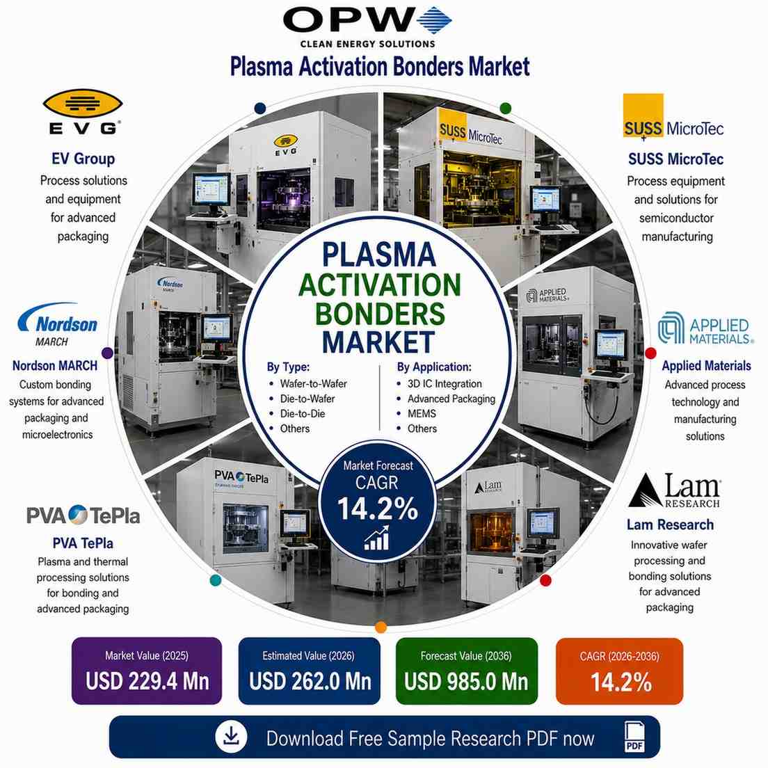
According to a comprehensive market research report published by Fact.MR, The global Plasma Activation Bonders Market crossed a valuation of $229.4 million in 2025 and is projected to expand from $262.0 million in 2026 to $985.0 million by 2036, recording a compound annual growth rate (CAGR) of 14.2% over the forecast period. This rapid adoption represents an absolute dollar opportunity of $723.0 million over the next decade.
Get detailed market forecasts, competitive benchmarking, and pricing trends: https://www.factmr.com/connectus/sample?flag=S&rep_id=15651
Market expansion is primarily driven by foundries and memory manufacturers scaling copper-dielectric hybrid bonding workflows, where creating highly reactive hydrophilic surfaces without plasma ion damage or particle contamination is essential to achieving reliable low-temperature wafer bonding.
Key Plasma Activation Bonders Market Highlights at a Glance
- Base Year Market Valuation (2025): $229.4 million
- Estimated Market Value (2026): $262.0 million
- Forecast Market Value (2036): $985.0 million
- Compound Annual Growth Rate (2026–2036):2%
- Absolute Dollar Opportunity (2026–2036): $723.0 million
- Leading Plasma Source Segment: N2 remote plasma with a 30.0% market share in 2026
- Leading Integration Mode Segment: Cluster-integrated activation with a 42.3% market share in 2026
- Leading Wafer Size Segment: 300 mm substrates commanding a 42.9% market share in 2026
- Leading Activation Target: Copper-dielectric (Cu-dielectric) hybrid surfaces
- Fastest-Growing National Market: Taiwan expanding at a 15.4% CAGR from 2026 to 2036
Why Is the Plasma Activation Bonders Market Growing?
Demand for plasma activation bonders is escalating as advanced semiconductor packaging transitions toward low-temperature direct bonding for high-density 3D integrated circuits. Three primary process drivers are accelerating tool adoption across commercial fabs:
- Creation of High-Density Hydrophilic Surfaces: Plasma exposure creates reactive dangling bonds and silanol (-OH) groups on silicon and dielectric surfaces, making them strongly hydrophilic and enabling strong van der Waals bonds upon room-temperature contact.
- Bypass of High Thermal Budgets: Pre-processed CMOS wafers cannot withstand bonding temperatures exceeding 600°C; plasma activation allows subsequent low-temperature annealing (150°C to 400°C) to convert initial contact into covalent Si-O-Si bonds.
- Elimination of Uncontrolled Ambient Air Exposure: Modern packaging flows require cluster-integrated tools to prevent activated reactive surfaces from decaying or attracting airborne molecular contamination before contact.
“Integrated activation-to-bond workflows will make surface activation a tightly controlled transfer step rather than an unmanaged process delay,” states Ganesh Pai, Lead Semiconductor Analyst at Fact.MR. “As chipmakers transition to sub-micrometer hybrid bond pitches, fabs must carefully balance plasma energy. Tooling that delivers remote nitrogen activation without physical ion-bombardment damage directly controls production yield in next-generation packaging lines.”
How Does the Market Break Down Across Major Segmentation Axes?
Plasma Source: Why N2 Remote Plasma Leads
N2 remote plasma is projected to account for a leading 30.0% market share in 2026. Remote nitrogen plasma supplies highly reactive radicals to the wafer interface while isolating delicate dielectric layers from direct ion bombardment.
- N2 remote plasma market share in 2026: 30.0%
- Primary process advantage: Supplies active radicals while avoiding physical ion-bombardment damage to surface dielectrics
- Key alternate segment: Direct Oxygen (O2) plasma, utilized for standard silicon-on-insulator (SOI) and silicon oxide fusion bonding
Integration Mode: Why Cluster-Integrated Activation Dominates
Cluster-integrated activation is forecast to command a 42.3% market share in 2026. Transferring activated wafers directly inside an isolated cluster tool eliminates ambient air exposure and prevents reactive silanol groups from decaying before wafer contact.
- Cluster-integrated activation market share in 2026: 42.3%
- Primary process advantage: Eliminates ambient queue-time decay and moisture reabsorption prior to optical alignment
- Key alternate segment: Standalone activation modules, deployed in lower-density packaging lines or batch research environments
Wafer Size: Why 300 mm Substrates Lead Production Volume
The 300 mm wafer size segment is projected to capture a 42.9% market share in 2026. High-volume logic foundries and HBM memory manufacturers rely exclusively on 300 mm wafer platforms for advanced packaging integration.
- 300 mm wafer size market share in 2026: 42.9%
- Process driver: Seamless integration into high-volume manufacturing infrastructure for leading-edge nodes
- Secondary segment: 200 mm wafer platforms, serving specialty analog, MEMS, and power semiconductor bonding lines
Activation Target & End User: Foundries Leading Cu-Dielectric Hybrid Bonding
Copper-dielectric (Cu-dielectric) hybrid surfaces represent the primary activation target, with pure-play foundries and memory makers driving tool procurement. Hybrid bonding requires synchronized activation of both silicon carbonitride (SiCN) dielectrics and copper contact pads.
- Primary activation target segment: Cu-dielectric hybrid surfaces and SiO2/SiCN dielectric films
- Primary end-user groups: Pure-play foundries and vertically integrated memory manufacturers
- Key application driver: Advanced logic chiplets, 3D stacked image sensors, and High-Bandwidth Memory (HBM) architectures
Plasma Activation Bonders Market Dynamics
Market Drivers
The primary market driver is the rapid transition toward low-temperature hybrid bonding in advanced packaging. Because fine-pitch interconnects cannot endure intense thermal processing, plasma surface activation is mandatory to achieve high bond strength at reduced annealing temperatures.
Market Restraints
Process sensitivity remains the principal market restraint. Over-activation can cause subsurface dielectric damage or polymer roughening, whereas under-activation results in weak bonding and interfacial voids, leading conservative fabs to mandate extended qualification periods.
Key Market Trends
A major trend is the development of fully automated cluster architectures that integrate megasonic cleaning, remote nitrogen plasma activation, and high-precision optical alignment within a continuous vacuum or controlled-nitrogen environment.
Regional and Country Outlook
Capital expenditure in plasma activation bonding equipment is heavily concentrated in East Asia, supported by dense foundry networks and aggressive memory packaging roadmaps.
- Taiwan CAGR (2026–2036):4%
- South Korea CAGR (2026–2036):0%
- United States CAGR (2026–2036):8%
- China CAGR (2026–2036):1%
- Japan CAGR (2026–2036):2%
Taiwan is projected to lead global market growth with a 15.4% CAGR through 2036. Growth is anchored by major semiconductor foundries expanding advanced packaging facilities, wafer-level chip-scale packaging lines, and substrate supply chains.
South Korea is forecast to expand at a 15.0% CAGR through 2036. Massive domestic investments in High-Bandwidth Memory (HBM) and next-generation DRAM stacking are driving demand for cluster-integrated plasma activation tools.
The United States, China, and Japan continue to demonstrate steady demand as government incentives accelerate onshore advanced packaging capacity for artificial intelligence processors and high-performance computing.
Competitive Landscape
The plasma activation bonders market is characterized by specialized semiconductor equipment providers focusing on defect reduction, process repeatability, and cluster integration.
- EV Group (EVG): Leading supplier of automated wafer bonding and surface activation systems with integrated cluster technology.
- SUSS MicroTec: Precision equipment manufacturer offering specialized surface processing and alignment modules for advanced packaging.
- Applied Materials: Global semiconductor equipment leader offering multi-chamber cluster platforms for surface preparation and deposition.
- Lam Research: Major equipment provider specializing in plasma etch, clean, and surface modification architectures.
- Nordson MARCH: Specialist in plasma surface treatment equipment tailored for microelectronics assembly.
- PVA TePla: Provider of microwave and RF plasma systems for wafer conditioning and surface activation.
Competitive dynamics center on delivering end-to-end process guarantees. Leading suppliers are forming joint development programs with packaging consortia to integrate plasma chemistry, cleaning, and bonding tools into unified high-yield packaging cells.
Read the Comprehensive Industry Report: https://www.factmr.com/report/plasma-activation-bonders-market
Frequently Asked Questions
What is the projected market size of the Plasma Activation Bonders Market by 2036?
The global Plasma Activation Bonders Market is projected to reach a valuation of $985.0 million by 2036.
What is the forecast growth rate (CAGR) for the Plasma Activation Bonders Market?
The Plasma Activation Bonders Market is forecast to grow at a compound annual growth rate (CAGR) of 14.2% from 2026 to 2036.
Which plasma source technology holds the largest share of the market?
N2 remote plasma represents the leading plasma source segment, holding a 30.0% market share in 2026.
What integration mode dominates plasma activation bonder installations?
Cluster-integrated activation is the dominant integration mode, capturing a 42.3% market share in 2026.
Which wafer size segment accounts for the highest market share?
The 300 mm wafer size segment commands the highest market share at 42.9% in 2026.
Which country is expected to be the fastest-growing market for plasma activation bonders?
Taiwan is forecast to be the fastest-growing national market, expanding at a 15.4% CAGR between 2026 and 2036.
Who are the key equipment manufacturers operating in this market?
Key market providers include EV Group, SUSS MicroTec, Applied Materials, Lam Research, Nordson MARCH, and PVA TePla.
To View Related Report:
Plasma Display Module Market: https://www.factmr.com/report/1885/plasma-display-module-market
In-Situ Overlay Bonders Market: https://www.factmr.com/report/in-situ-overlay-bonders-market
Queue-Time Hybrid Bonders Market: https://www.factmr.com/report/queue-time-hybrid-bonders-market
Backside Via Inspection Market: https://www.factmr.com/report/backside-via-inspection-market
To View More Report:
Queue-Time Hybrid Bonders Market: https://www.openpr.com/news/4585592/u-s-queue-time-hybrid-bonders-market-besi-expands-advanced
Plasma Activation Bonders Market: https://www.openpr.com/news/4585599/asia-pacific-leads-plasma-activation-bonders-market-as-ev-group