Market expands at 12.6% CAGR as deep channel-hole etching and 3D NAND layer scaling increase demand for cryogenic etch systems
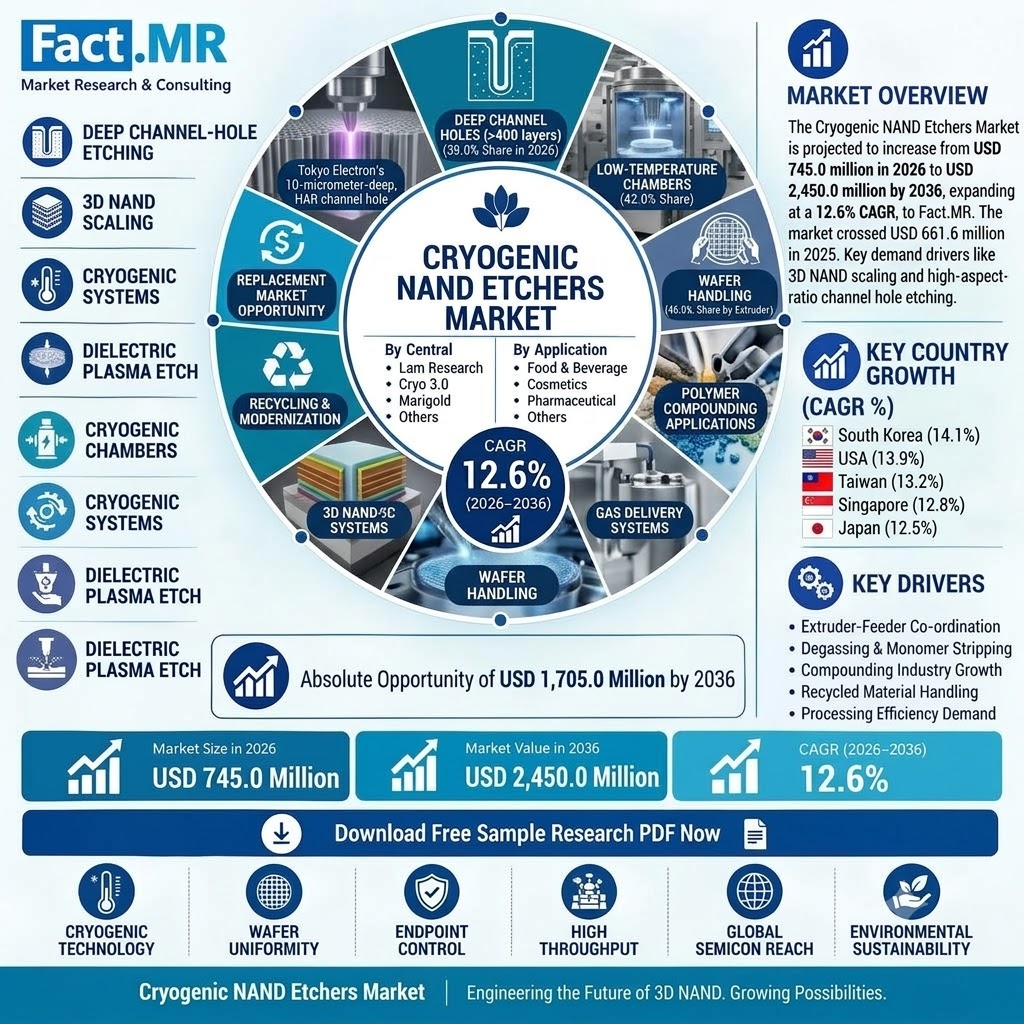
The Cryogenic NAND Etchers Market is projected to increase from USD 745.0 million in 2026 to USD 2,450.0 million by 2036, expanding at a 12.6% CAGR, according to Fact.MR analysis. The market crossed USD 661.6 million in 2025 as NAND manufacturers sought process technologies capable of etching deep, narrow channel holes through hundreds of alternating dielectric layers without bow, taper or bottom starvation.
The market is expected to create a USD 1,705.0 million absolute opportunity by 2036. Demand is being shaped by the increasing difficulty of conventional reactive ion etching as channel-hole depth rises, alongside advances in cryogenic dielectric etch technology from major semiconductor equipment suppliers.
Get detailed market forecasts, competitive benchmarking, and pricing trends: https://www.factmr.com/connectus/sample?flag=S&rep_id=15665
Cryogenic NAND Etchers Market gains momentum from deep-channel etching
Fact.MR identifies cryogenic etching as a response to a specific process limitation. In conventional RIE, etch rate declines with depth in tiny channel holes. Cryogenic operation suppresses unwanted sidewall etching while enhancing ion mobility and bombardment, using platform chillers and helium wafer cooling to achieve ultra-low wafer temperatures.
A key technical reference is Tokyo Electron Miyagi’s cryogenic dielectric etch work presented at VLSI 2023. The technology etched a 10-micrometer-deep, high-aspect-ratio channel hole in 33 minutes for stacks exceeding 400 layers. The same work reported an 84% reduction in global-warming potential compared with the previous generation through substitution of HF-based chemistry for high-GWP CF gases.
That result has become an important reference point for the market. Lam Research is also positioning Cryo 3.0 for future 3D NAND devices at 400 layers and beyond, with compatibility across Flex and Vantex conductor and dielectric etch platforms used in high-volume manufacturing.
Fact block: Fact.MR defines cryogenic NAND etchers as dielectric plasma etch systems that operate at wafer temperatures well below 0°C to etch oxide/nitride memory channel holes and staircase structures in 3D NAND. The market scope covers cryogenic etch chambers, low-temperature control, gas delivery, RF systems, wafer handling, endpoint control and application support.
Channel-hole etch holds the largest application share
Channel-hole etch is projected to account for 36.0% of the market in 2026, making it the leading segment by etch application. The process passes through hundreds of alternating dielectric layers while maintaining profile accuracy, selectivity and access to the feature bottom.
The -20°C to -40°C operating range is forecast to hold 39.5% share in 2026. Features below 40:1 aspect ratio are projected at 38.6%, while single-wafer chambers are estimated to account for 42.9%. NAND manufacturers are expected to represent 33.3% of the market in 2026.
These figures reflect the practical requirements of production. Single-wafer chambers allow direct control over wafer temperature, plasma conditions and endpoint detection, which becomes increasingly relevant when etch performance depends strongly on surface temperature.
Qualification remains a key production challenge
Market expansion is not without technical constraints. Fact.MR identifies maintaining uniform cryogenic temperature and chemistry across a 300 mm wafer as a primary qualification challenge because it adds chamber and endpoint-control complexity. Throughput sensitivity and thermal or mechanical distortion are also identified as restraints.
Scaling beyond 400 layers introduces further process challenges. Counterpoint analysis cited in the report frames 1,000-layer 3D NAND as a future scaling horizon, with slower etch rates and vertical-profile variability requiring continued advances in etch, deposition and polymer management.
Shambhu Nath Jha, Sr. Consultant at Fact.MR, said, “Buyers should evaluate the complete process sequence around etching deep, narrow channel holes through hundreds of alternating dielectric layers without bow, taper or bottom starvation. Technical review should focus on repeatability, integration, defect control and production throughput rather than a single headline specification.”
South Korea records the highest projected country CAGR
South Korea is projected to record a 14.1% CAGR from 2026 to 2036, supported by high-volume memory, HBM and vertically integrated semiconductor manufacturing. The USA follows at 13.9%, Taiwan at 13.2%, Singapore at 12.8% and Japan at 12.5%.
The country outlook reflects different semiconductor production structures. South Korea’s demand is linked to memory and HBM manufacturing, while the USA combines leading-edge logic, high-performance computing, semiconductor R&D and a domestic equipment base. Taiwan’s market is associated with foundry production and advanced packaging, while Japan draws on semiconductor equipment, materials, inspection and memory-process expertise.
Competitive landscape
Lam Research and Tokyo Electron are identified as leading participants in the competitive landscape, followed by Applied Materials and Hitachi High-Tech. The report states that competition centers on repeatable process performance, integration with adjacent modules, installed-base service and documented capability in deep channel-hole etching.
“Qualification must balance etch rate, profile control, selectivity, wafer temperature stability and chamber productivity,” said Shambhu Nath Jha, Sr. Consultant at Fact.MR. “The production question is not just how fast a tool etches. It is whether the process stays repeatable across representative wafers and integrates with the wider 3D NAND flow.”
Top Reports :
About Fact.MR
Fact.MR is a market research and consulting company providing market intelligence across technology, industrial, chemicals, automotive, healthcare and other sectors. Its research combines market assessment, public company disclosures, government and regulatory publications, technical literature, trade information and industry records. The Cryogenic NAND Etchers Market report covers the 2026–2036 forecast period across etch application, operating temperature, aspect ratio, chamber configuration, end user and country-level growth.