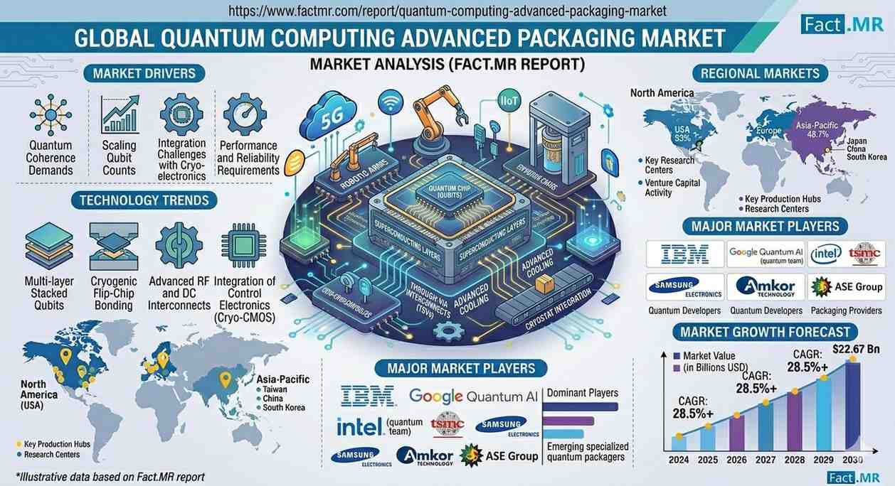
The global Quantum Computing Advanced Packaging market is positioned for a decade of high-intensity technical evolution, projected to grow from USD 91.10 million in 2026 to USD 278.65 million by 2036. This represents a robust compound annual growth rate (CAGR) of 11.8%, according to the latest strategic analysis.
As quantum processors transition from isolated laboratory experiments to integrated, multi-qubit systems, conventional integrated circuit (IC) packaging has proven inadequate. The market is now being defined by a “Cryo-Ready” revolution, where packaging must manage extreme thermal gradients, provide dense interconnects, and protect fragile quantum states from environmental noise.
Executive Market Summary (2026–2036)
- 2026 Valuation: USD 91.10 Million
- 2036 Projection: USD 278.65 Million
- Absolute Growth:8%
- Dominant Architecture:5D Interposer (48% Market Share)
- Lead Qubit Modality: Superconducting (45% Market Share)
The Critical Bottleneck: Why Advanced Packaging?
Quantum Advantage is no longer just a physics challenge; it is a packaging challenge. Advanced packaging provides the essential interface between the quantum world (operating at millikelvin temperatures) and classical control electronics.
- Thermal Management: Packaging must endure extreme cryogenic cycling without mechanical failure or signal degradation.
- I/O Density: Scaling to thousands of qubits requires thousands of control and readout lines, necessitating the shift toward 5D Interposers and Wafer-Level Packaging.
- Signal Integrity: Minimizing electromagnetic interference (EMI) is paramount to preserving qubit coherence.
Segmental Analysis: 2.5D Interposers and Superconducting Dominance
The 2.5D Interposer segment leads the market with a 48% share in 2026. This architecture allows for the side-by-side integration of quantum processor dies and classical ASICs, providing the short-path interconnects vital for high-fidelity operations.
From a modality perspective, Superconducting qubits remain the primary demand driver (45% share), as industry giants like IBM and Google scale their “gate-based” systems, requiring increasingly complex cryogenic wiring and shielding solutions.
Regional Outlook: The Global Race for Quantum Sovereignty
Regional growth is highly concentrated in hubs where government-backed research meets private semiconductor expertise.
| Country | Projected CAGR (2026-2036) | Strategic Advantage |
| Netherlands | 13.1% | Hub for spin-qubit research (QuTech) and ASML-linked ecosystems. |
| USA | 12.4% | Concentration of Big Tech (Google, IBM) and National Labs. |
| Japan | 12.1% | World-class precision ceramics and low-temp materials engineering. |
| Germany | 11.4% | Emphasis on industrial-grade engineering and standardized protocols. |
Competitive Landscape: The Entrance of Foundries and OSATs
The market is currently characterized by a “High-Value, Low-Volume” model, where established semiconductor leaders are forming deep strategic partnerships with quantum innovators.
- Foundries (TSMC, Intel, Samsung): Leveraging their advanced node capabilities to offer full-stack quantum-classical integration.
- OSATs (ASE, Amkor, JCET): Adapting existing advanced packaging toolkits for cryogenic reliability and ultra-pure material requirements.
Actionable Insights for Decision-Makers
Investment Opportunities
- Cryo-Compatible Materials: Significant upside exists for suppliers of low-loss dielectrics and ultra-pure substrates capable of withstanding millikelvin environments.
- Co-Design Software: There is a critical gap for EDA (Electronic Design Automation) tools that can simultaneously simulate quantum physics and classical thermal/electrical stresses within a single package.
Market Risks
- Lack of Standardization: The fragmentation of qubit modalities (Superconducting vs. Photonic vs. Ion Trapped) prevents the achievement of economies of scale in packaging.
- Cost of Failure: A single packaging defect in a multi-million dollar quantum system can lead to months of experimental delays.
Future Outlook: From Lab to Fab
By 2036, the market will shift from bespoke, hand-assembled packages toward automated Chiplet-Based modular platforms. This transition will be essential for the commercialization of Fault-Tolerant Quantum Computing, turning advanced packaging from a research bottleneck into a high-throughput industrial enabler.
Browse Full Report –
https://www.factmr.com/report/quantum-computing-advanced-packaging-market