The global semiconductor industry is entering a decisive decade as advanced process nodes, artificial intelligence (AI), and escalating design complexity converge. Among the most critical enablers of this transition are AI-driven Electronic Design Automation (EDA) tools optimized for 3nm process technology. Between 2026 and 2036, the 3nm semiconductor EDA AI tools market is expected to emerge as a high-value, strategic segment supporting next-generation logic, AI accelerators, high-performance computing (HPC), and advanced mobile systems.
Market Size and Growth Outlook
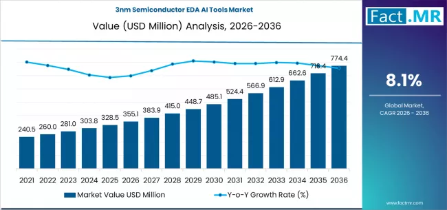
The global 3nm semiconductor EDA AI tools market is valued at approximately USD 380 million in 2026 and is projected to reach USD 830–840 million by 2036, expanding at a compound annual growth rate (CAGR) of around 8.1% over the forecast period. While the absolute market size remains modest compared with the overall EDA market—projected to exceed USD 25 billion by 2030—the strategic importance of 3nm-focused AI tools is disproportionately high. These solutions sit at the intersection of foundry roadmaps, fabless innovation, and AI-driven semiconductor demand.
Strategic Drivers Shaping Demand
1. Escalating Design Complexity at 3nm
At 3nm, traditional rule-based EDA approaches struggle to manage exploding design variables, tighter power-performance-area (PPA) trade-offs, and yield risks. AI-enhanced place-and-route (P&R), logic synthesis, verification, and sign-off tools are increasingly essential to reduce design cycles and improve first-silicon success. P&R and synthesis tools alone account for roughly 30–31% of total market share, making them the largest functional segment in the 3nm EDA AI tools landscape.
2. Foundry-Led Adoption
Foundries represent the dominant customer segment, contributing approximately 44% of total demand for 3nm EDA AI tools. Leading foundries are investing heavily in design-technology co-optimization (DTCO), requiring AI-driven EDA platforms tightly integrated with process development kits (PDKs). This trend is reinforced by continued capacity expansion in advanced nodes, even as overall foundry utilization stabilizes near 70% globally through 2030.
3. AI-Driven Semiconductor Demand
The rapid expansion of AI workloads is reshaping semiconductor economics. AI, cloud, and mobility applications will push the broader semiconductor market toward USD 1 trillion in annual revenue by 2030, with advanced nodes below 3nm playing a central role. As AI chips grow larger and more complex, AI-assisted EDA becomes indispensable to protect yield, manage power density, and control design costs.
Innovation Trends in EDA AI Tools
Machine Learning-Based Optimization:
Next-generation EDA platforms increasingly rely on machine learning models trained on millions of design iterations to predict routing congestion, power hotspots, and timing violations earlier in the design flow. This reduces costly late-stage rework and shortens time-to-market—an issue where a single design slip at advanced nodes can translate into losses exceeding USD 100 million.
AI-Driven Verification and Sign-Off:
Verification complexity grows exponentially at 3nm due to tighter margins and heterogeneous integration. AI-based verification tools can prioritize high-risk design paths, cutting verification cycles and compute costs while improving coverage.
Power, Thermal, and Yield Intelligence:
AI-enabled power and thermal analysis tools are gaining traction as advanced nodes face rising leakage currents and heat density. Yield optimization solutions using predictive analytics help designers and foundries identify manufacturability risks before tape-out, directly supporting profitability.
Regional and Ecosystem Dynamics
Asia-Pacific remains the epicenter of 3nm development, driven by Taiwan, South Korea, and increasingly China. Semiconductor equipment spending is forecast to rise sharply, largely fueled by AI-related investments in advanced logic and memory. This capital intensity directly benefits EDA vendors supplying AI-driven tools aligned with leading-edge process nodes.
At the same time, geopolitical considerations and government incentives in the U.S. and Europe are encouraging localized design and manufacturing capabilities. These initiatives are expected to support incremental demand for advanced EDA solutions over the 2026–2036 period.
Growth Opportunities Through 2036
The next decade presents several high-value opportunities for vendors and stakeholders:
- Deep Integration with Foundry Roadmaps: EDA providers that align AI models closely with specific 3nm and post-3nm processes will gain long-term competitive advantages.
- Subscription and Usage-Based Licensing: Flexible commercial models are lowering barriers for fabless and IDM customers, accelerating adoption of AI-driven tools.
- Expansion Beyond 3nm: Capabilities developed for 3nm will be transferable to 2nm and advanced packaging workflows, extending revenue potential beyond the forecast horizon.
- Ecosystem Partnerships: Collaboration between EDA vendors, foundries, and cloud providers will be critical to scale compute-intensive AI design flows efficiently.
Browse Full Report : https://www.factmr.com/report/3nm-semiconductor-eda-ai-tools-market
Outlook
From 2026 to 2036, the global 3nm semiconductor EDA AI tools market will evolve from a specialized niche into a strategic cornerstone of advanced semiconductor innovation. With steady 8%+ annual growth, strong foundry demand, and accelerating AI-driven chip complexity, these tools will play a decisive role in shaping the economics and competitiveness of the semiconductor industry over the next decade.