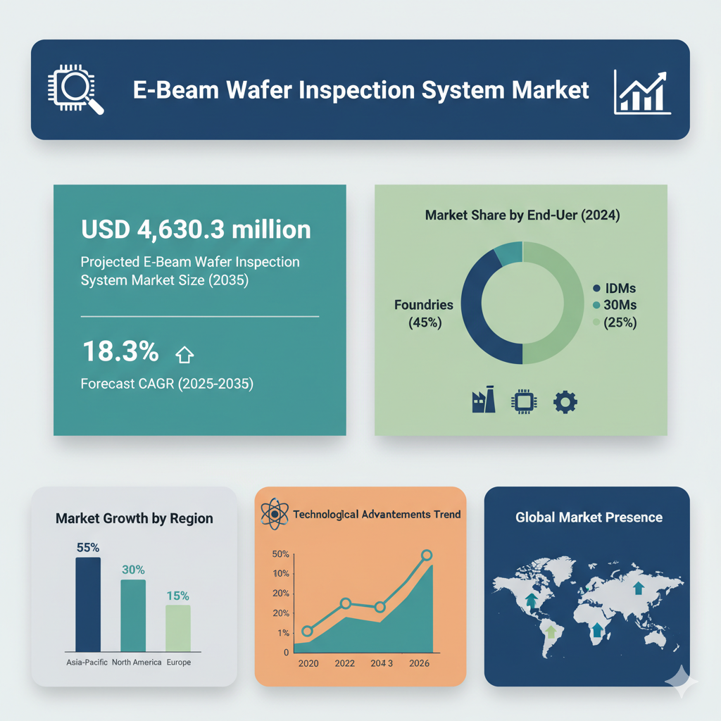
The global e-beam wafer inspection system market is projected to increase from USD 862.5 million in 2025 to USD 4,630.3 million by 2035, with a CAGR of 18.3 % during the forecast period. This remarkable growth reflects the rising demand for precision semiconductor inspection systems capable of detecting the smallest defects as chip architectures become increasingly complex. The e-beam (electron beam) wafer inspection technology plays a vital role in ensuring high-yield production, particularly as semiconductor nodes advance below 10 nm and the industry shifts toward 3D structures and heterogeneous integration.
Market Segmentation Overview
The e-beam wafer inspection system market is segmented by type, wafer node, application, end-user, and region. Based on type, the market is divided into single-beam and multi-beam systems. While single-beam systems currently hold a significant share due to their established use in mature node processes, multi-beam systems are rapidly gaining traction because they offer much higher throughput, making them ideal for advanced wafer nodes and high-volume manufacturing environments.
By wafer node, the market is categorized into mature nodes (above 10 nm) and advanced nodes (10 nm, 7 nm, 5 nm, and below). The demand for inspection systems in advanced nodes is expected to surge as manufacturers push toward smaller geometries that require more sophisticated defect detection and pattern analysis capabilities. Mature nodes, however, will continue to see steady demand from sectors such as automotive and industrial electronics, where performance and cost efficiency are prioritized over extreme miniaturization.
In terms of application, logic chips and memory chips represent the two largest categories. Logic chips, used in processors and SoCs, require constant inspection innovation to maintain performance and reliability. Memory chips, including DRAM and NAND, drive significant equipment investments as manufacturers strive to reduce defect rates and improve yields. Other applications, such as specialty semiconductors and power devices, also contribute to market expansion as semiconductor usage broadens across industries.
The end-user segmentation includes automotive, consumer electronics, IT and telecom, industrial, and others. Consumer electronics remains the leading segment, supported by the continuous evolution of smartphones, wearables, and high-performance computing devices. Automotive applications are experiencing rapid growth as electric vehicles and advanced driver-assistance systems demand higher chip reliability and precision. IT and telecom industries are also key consumers, especially as 5G and data-center expansion accelerate the need for advanced semiconductor components. Regionally, Asia-Pacific dominates the market due to the concentration of foundries and fabrication facilities in countries such as China, Japan, Taiwan, and South Korea. North America and Europe are also important markets, driven by technological innovation, government incentives, and the establishment of new semiconductor manufacturing plants.
Recent Developments and Driver Trends
Recent years have witnessed major technological advancements in e-beam wafer inspection systems, with manufacturers focusing on increasing throughput, resolution, and automation. The integration of artificial intelligence and machine learning into inspection tools has enabled faster defect classification, reduced false positives, and enhanced overall process control. These innovations are crucial as chip manufacturers move toward sub-5 nm nodes and 3D architectures, where traditional optical inspection methods are no longer sufficient.
Global investments in semiconductor manufacturing are another key driver of market expansion. Governments in the United States, China, Japan, and the European Union have launched significant funding initiatives to strengthen domestic chip production capabilities, directly boosting demand for inspection equipment. Moreover, the growing complexity of automotive electronics, 5G infrastructure, and Internet of Things (IoT) devices continues to stimulate the need for precise and scalable wafer inspection technologies.
In addition, the industry has seen a steady increase in collaborations and partnerships between equipment vendors and semiconductor foundries. These alliances aim to co-develop next-generation inspection solutions optimized for specific fabrication processes and packaging technologies, including 3D stacking and chiplet architectures.
Key Players and Competitive Landscape
The e-beam wafer inspection system market features several leading players, including ASML Holding N.V., Applied Materials Inc., Hitachi Ltd., KLA Corporation, HOLON Co. Ltd., and MKS Instruments Inc. These companies are continuously investing in R&D to enhance their inspection systems’ speed, accuracy, and cost efficiency.
KLA Corporation remains one of the dominant forces in process control and inspection, leveraging decades of experience in wafer defect detection. ASML, through its HMI division, integrates e-beam inspection technologies into its lithography ecosystem, offering comprehensive solutions for advanced chip production. Applied Materials focuses on developing scalable inspection platforms that integrate advanced analytics and software for predictive defect analysis. Hitachi, with its deep expertise in electron microscopy, continues to develop high-resolution systems suited for both research and production environments.
The competitive landscape is moderately concentrated, with established players maintaining strong global presence. However, increasing demand for multi-beam inspection systems and AI-driven tools is creating opportunities for new entrants specializing in niche technologies and custom solutions.
Strategic Insights and Market Outlook
Companies that can deliver high-throughput, cost-efficient, and AI-enabled inspection solutions are expected to gain a significant competitive advantage. The market’s growth is further supported by the expansion of semiconductor fabrication facilities in emerging economies, as well as the integration of advanced packaging and 3D chip designs, which demand precise inspection capabilities at every production stage.
Challenges persist, however. The high cost of e-beam inspection systems and the need for specialized operational expertise may limit adoption among smaller manufacturers. Additionally, as optical inspection continues to evolve, e-beam vendors must clearly demonstrate superior value and performance to justify the investment.
Looking ahead, the e-beam wafer inspection system market will play a crucial role in enabling the semiconductor industry’s next wave of innovation. With robust growth projected from USD 862.5 million in 2025 to USD 4,630.3 million by 2035, the market’s future hinges on technological evolution, strategic partnerships, and regional manufacturing expansion. Vendors that successfully integrate cutting-edge technology with scalable production support will lead the next generation of semiconductor inspection solutions.