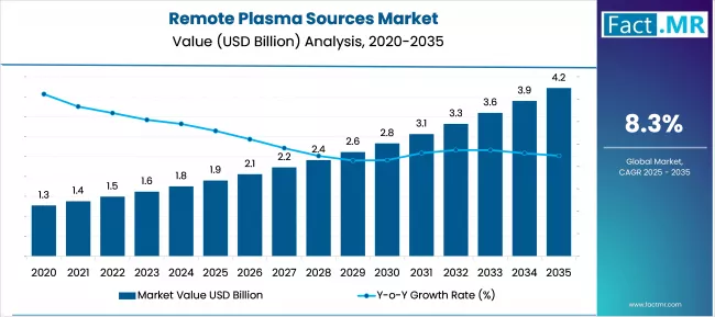
The global remote plasma sources market is on track for significant growth over the next decade. Valued at approximately USD 1.9 billion in 2025, the market is forecast to more than double—to around USD 4.2 billion by 2035—with a projected compound annual growth rate (CAGR) of about 8.3%. This growth trajectory reflects strong demand from semiconductor manufacturing, advanced surface treatment, and thin-film applications, among other sectors.
Key Growth Drivers
-
Surging Semiconductor Demand
Remote plasma sources (RPS) play a critical role in semiconductor fabrication by enabling ultra-clean etching, wafer cleaning, and plasma-enhanced deposition. As chipmakers push for smaller geometries, higher densities, and defect-free surfaces, the need for precision plasma control continues to rise. -
Miniaturization and Advanced Packaging
As integrated circuits shrink and advanced packaging (such as 3D ICs or through-silicon vias) becomes more common, manufacturers increasingly rely on RPS to treat delicate surfaces without damaging underlying structures. The non-destructive nature of remote plasma makes it ideal for these precision processes. -
Thin Film Deposition and Surface Treatment
Remote plasma sources support critical processes like ALD (atomic layer deposition), PECVD (plasma-enhanced chemical vapor deposition), and specialized thin-film coating. These techniques are now widely used not only in semiconductors, but also in MEMS, optics, solar cells, and other advanced materials. -
Environmental and Process Efficiency
Compared to wet chemical methods, plasma-based processes can reduce chemical waste, lower hazardous byproducts, and improve process control. This makes remote plasma particularly attractive as companies and governments push for cleaner, more sustainable manufacturing methods. -
Adoption of Smart Manufacturing
Next-generation plasma systems are increasingly being integrated with IoT, real-time process monitoring, and predictive maintenance. These smart systems reduce downtime, optimize gas consumption, and offer superior quality control.
Technology Landscape
-
Inductively Coupled Plasma (ICP) is expected to remain a dominant technology within remote plasma sources due to its high plasma density, uniformity, and compatibility with high-precision processing.
-
Microwave Plasma Sources and other advanced plasma technologies are also gaining ground as manufacturers demand even greater control, lower contamination risk, and higher energy efficiency.
To Access the Complete Data Tables & in-depth Insights, Request a Discount on this report: https://www.factmr.com/connectus/sample?flag=S&rep_id=11204
Application Segments
-
Semiconductor Manufacturing: This remains the single largest application, especially for wafer cleaning and etching. As semiconductor fabs scale up and adopt more advanced nodes, they increasingly invest in remote plasma systems to improve yield and device reliability.
-
Thin-Film Deposition: Remote plasma enables conformal and uniform coatings for a range of applications—such as electronic displays, solar cells, and sensor devices.
-
Surface Treatment and Cleaning: Beyond semiconductors, remote plasma is widely used for activating, cleaning, and treating surfaces in industries such as aerospace, automotive, and advanced materials.
Regional Dynamics
-
Asia-Pacific: The region is projected to lead the market, driven by massive semiconductor capacity build-outs, electronics manufacturing, and government support for high-tech infrastructure.
-
North America: Strong innovation in plasma technologies, combined with established semiconductor ecosystems, is expected to fuel robust growth.
-
Europe: Growth is supported by industrial modernization, precision manufacturing, and demand from surface engineering and specialty material sectors.
Challenges & Restraints
-
High CapEx: Remote plasma systems are capital-intensive. Many manufacturers, especially smaller fabs or emerging regions, may be deterred by the high initial cost of adoption.
-
Integration Complexity: Implementing RPS into existing manufacturing lines can be technically challenging and may require significant adjustments or upgrades to current infrastructure.
-
Skills Gap: Running and maintaining advanced plasma systems requires expertise. Specialized training and skilled personnel remain a barrier for many companies.
-
Competition: Alternative plasma technologies, as well as non-plasma-based cleaning or deposition methods, can reduce the reliance on remote plasma in certain applications.
Strategic Implications
-
For Equipment Manufacturers: Investment in R&D is critical. Companies should focus on energy-efficient plasma sources, high-density systems, smart control platforms, and modular designs that lower upfront costs.
-
For Semiconductor Producers: Upgrading to remote plasma systems can improve process quality, reduce contamination, and ultimately enhance chip yield. Collaboration with plasma-source providers can unlock tailored solutions.
-
For Industrial Processors: Companies in coatings, aerospace, or advanced materials should evaluate RPS for surface activation, corrosion resistance, and performance enhancement.
-
For Investors: The market’s strong long-term growth potential, driven by semiconductor and green-manufacturing megatrends, presents a compelling investment opportunity in plasma technology suppliers and integrators.
Competitive Landscape
Key players in the remote plasma sources market include major instrumentation, semiconductor, and materials-equipment companies. Competition is primarily based on technological innovation, reliability, integration support, and post-sale service. Leaders are differentiating through intelligent plasma controls, modular platforms, and global support networks.
Outlook Summary
Over the next decade, the remote plasma sources market is expected to more than double, underpinned by growing semiconductor demand, increasing surface-treatment needs, and the shift toward cleaner, more precise manufacturing techniques. While challenges around cost, integration, and talent persist, companies that offer efficient, high-density, and smart plasma systems are well positioned to lead the market. As RPS becomes central to advanced fabrication and materials processing, its adoption will likely become a key pillar of next-generation manufacturing infrastructure.
Have specific requirements or need assistance on report pricing or have a limited budget? Please contact sales@factmr.com
Contact:
US Sales Office
11140 Rockville Pike
Suite 400
Rockville, MD 20852
United States
Tel: +1 (628) 251-1583, +353-1-4434-232
Email: sales@factmr.com
About Fact.MR:
Fact.MR is a global market research and consulting firm, trusted by Fortune 500 companies and emerging businesses for reliable insights and strategic intelligence. With a presence across the U.S., UK, India, and Dubai, we deliver data-driven research and tailored consulting solutions across 30+ industries and 1,000+ markets. Backed by deep expertise and advanced analytics, Fact.MR helps organizations uncover opportunities, reduce risks, and make informed decisions for sustainable growth.